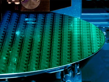
Advancing Connectivity with KLA’s New IC Substrate Product Portfolio
KLA revamped its intelligent portfolio of solutions for IC substrates with several product updates. Advanced packaging continues to adopt heterogeneous...

Our process-control and process-enabling solutions are designed to boost the innovation speed of the electronics industry. We help our customers achieve leading-edge performance.
KLA revamped its intelligent portfolio of solutions for IC substrates with several product updates. Advanced packaging continues to adopt heterogeneous...
Innovation is diversifying in the semiconductor chip industry, resulting in new approaches to meet the performance needs of advanced technologies...
In today’s digital world, the extensive use of electronic devices and accelerating use of AI drive demand for a diverse...
KLA’s new Axion® T2000 metrology system harnesses the power of X-rays to measure the complex vertical structures that form advanced memory chips....
The new Orbotech Corus™ 8M direct imaging (DI) system is the first solution built on KLA’s all-in-one revolutionary Orbotech Corus...
Today’s chip manufacturers contend with strict requirements when it comes to quality assurance, since more complex chips are powering increasingly...
You've selected to view this site translated by Google Translate.
KLA China has the same content with improved translations.
Would you like to visit KLA China instead?
您已选择查看由Google翻译翻译的此网站。
KLA中国的内容与英文网站相同并改进了翻译。
你想访问KLA中国吗?
If you are a current KLA Employee, please apply through the KLA Intranet on My Access.